EAGLE FOR BEGINNERS
In my last post we had gone through a basic light triggering circuit Hope you are happy with your first "TechProject"now lets go one step ahead and we will learn the basics of a PCB designing software "EAGLE".
After this you can actually design a circuit of your own and get rid of those messy SOLDER'S and WIRE'S and give your circuit a professional look.
Lets GET started
So Eagle is basically a software that can be used to design your PCB(printed circuit board) that can be latter printed either at home or can be printed at some pcb printing shop to get more professional and accurate.
STEPS:
- Download and install Eagle.eagle is not a free software but you can get the lite version for free which is sufficient as of now. you can get the eagle lite version at the below link: http://www.cadsoftusa.com/download-eagle/freeware/
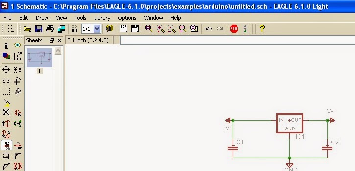
- Open the eagle software,Following screen will appear on the desktop.

3. Now click on File and then new and then open schematic.

4. Then the following window will appear before you
The schematic is a place where you can add your components and then make the connections as you do normally in any simulation software or say as the circuits you make in your book.You can see a simple schematic of voltage regulator in the image.
5. COMMANDS:
Now lets look at the important commands that will be usefull while designing the schematic

- MOVE:
The move command is used to move the component in the schematic frame and arrange the components as required .It should be noted that the arrangement of componet in the schematic is not so important as the final arrangement is done in the board file only, the schematic is just for reference.
- ADDING COMPONETS IN THE SCHEMATIC:
 This command can be found in the tray on the left of the screen click this to add new componets ,Clicking ADD open the following window.
.bmp)
Then click on the componet required and then Click OK to add the component in the schematic.
- WIRING UP:
 Now after adding the componets you need to wire them up you will see the LINE icon on the tray clicking it enable the wire and then using your mouse you can connect the wire between required terminals.
6. LOADING LIBRARIES:
Click on 'LIBRARY' tab and then 'USE' the select all the libraries and then add them .This needs to be done when you open Eagle for the first time.
- ADDING NEW LIBRARIES: Click on 'LIBRARY' then 'USE' you can then find the link of the lbr folder on your PC
- Place the dowloaded lbr file in this folder and then restart Eagle ,if required you may need to load the library for first time by following the procedure above.
Now you are ready to design your own circuit.
THIS ARE THE BASIC COMMAND THAT YOU NEED TO NOW IF YOU ARE A BEGINNER IN EAGLE THEN THE REST CAN BE LEARNT AS YOU GO ON PRACTICING BY DESIGNING NEW CIRCUITS IN EAGLE .
Now you are ready to design your own circuit
HOPE THIS HELPS!!!!!!!!!!!!!!!!!!!
THANKYOU
EAGLE PCB DESIGNING TUTORIALS FOR BEGINNERS-2(6-STEPS)
- MOVE:
The move command is used to move the component in the schematic frame and arrange the components as required .It should be noted that the arrangement of componet in the schematic is not so important as the final arrangement is done in the board file only, the schematic is just for reference.
- ADDING COMPONETS IN THE SCHEMATIC:
This command can be found in the tray on the left of the screen click this to add new componets ,Clicking ADD open the following window.- WIRING UP:
Now after adding the componets you need to wire them up you will see the LINE icon on the tray clicking it enable the wire and then using your mouse you can connect the wire between required terminals.
6. LOADING LIBRARIES:
Click on 'LIBRARY' tab and then 'USE' the select all the libraries and then add them .This needs to be done when you open Eagle for the first time.
- ADDING NEW LIBRARIES: Click on 'LIBRARY' then 'USE' you can then find the link of the lbr folder on your PC
- Place the dowloaded lbr file in this folder and then restart Eagle ,if required you may need to load the library for first time by following the procedure above.
THIS ARE THE BASIC COMMAND THAT YOU NEED TO NOW IF YOU ARE A BEGINNER IN EAGLE THEN THE REST CAN BE LEARNT AS YOU GO ON PRACTICING BY DESIGNING NEW CIRCUITS IN EAGLE .
Now you are ready to design your own circuit
HOPE THIS HELPS!!!!!!!!!!!!!!!!!!!
THANKYOU
In the previous post we had gone through the basic of designing a circuit in eagle basically schematic,now we will learn a more interesting part in eagle that is actually designing the "BOARD". Your board file actually determines the way your circuit will look.
Hope you have eagle installed and have made a simple schematic of any circuit that may be yours or from the internet ,now we will learn how to convert this simple schematic into a aPCB.
1) Open the .sch file that you have created using EAGLE.
2) Now click on FILE and then click on "Switch to Board" it will ask whether to create a new .brd file then click on yes it will we saved in the same folder as the schematic(.sch) file.
3) The following window will appear.It will have all the components placed outside the board shown with withe line.
.bmp)
1) Open the .sch file that you have created using EAGLE.
2) Now click on FILE and then click on "Switch to Board" it will ask whether to create a new .brd file then click on yes it will we saved in the same folder as the schematic(.sch) file.
3) The following window will appear.It will have all the components placed outside the board shown with withe line.
4) Using the group and move commands move all the components inside the board(the board is shown with a white rectangle on the screen).
.bmp)
.bmp) |
| GROUP THE COMPONENTS |
.bmp) |
RIGHT CLICK AND SELECT MOVE GROUP.bmp) DONE!!!
5) Arrange the components as required on the board.
.bmp) Let us now have a look at some important commands that would be useful further. |
- LAYER: This icon contains the list of all the layers and there colour on the board ,the layer can be either made visible or invisible by selecting them. A blue mark on the side indicates the layer is visible.This is usefull while printing ,in which we don't want all the layers but only three layers are required like TOP,PADS VIAS and BOTTOM if you have any text or dual sided PCB

- AUTOROUTE: This is the command you would love to use because it does most of the designing work for us but sometimes not all the work.This command tries all the possible combination of connecting the terminals and find a optimum path for us.
what do you think about this!!!!!!
.bmp)
Auto-Route worked for me this time!!!!!!!!!!!
.bmp)
- RATSNEST: This command tells us if there are any air wires in the circuit.Air wires are the wire that are not routed in the board file.
- ERC(Electrical rule check): This shows all the electrical errors that are there in the circuit like clearance between two paths and drill size etc.
Now lets get back to work
6) We had come up-to the 5th step i.e Our componets are now arranged on the board now lets try "ROUTING" them. Routing is nothing but as the name suggest a route or path of copper between two terminals which are to be connected to each other.So since in our circuit we have many terminals there are many routes as well, Thus as the size of the circuit increases the number of route increases,increasing the complexity of the circuit so what comes handy at such situations is the "AUTO ROUTING" command which has been discussed and hope you are familiar with it now.
So now lets AUTO-ROUTE:
.bmp)
You may think it is done but no it is not.It still requires some finishing because while printing the circuit there are some physical constraints.you should move the adjacent wires apart and maintain a safe distance between them and see to it that while printing they are not very close to each other.
can you see the changes i have made??? just use the move command and move the wires as you want.
.bmp)
So finally you have designed your own customized PCB.
In the next post i will take you through the process of printing this PCB on the screen to actual paper with proper "DIMENSIONS"
HOPE THIS HELPS.
.bmp)
In this method we directly take the print of the file and thus have only a single PCB on a page.
.bmp)
.bmp)
.bmp)
.bmp)

.bmp)
EAGLE PCB DESIGNING TUTORIALS FOR BEGINNERS-3
PRINTING IT ON THE PAPER:
In
the Previous segment of this series of eagle post we had come uptil the
eagle board file of the circuit, Now in this post we will go through
the steps to be followed before we transfer this .brd file on a actual
board.
1) open the board file we have designed and now we need to do some settings before we actually print this on a paper.
2) Your .brd file would look something like this.
But
if we take the print directly the components that are visible will also
get printed on the paper and thus will cause unnecessary shorts in the
circuit.To prevent this we need to eliminate the components from the brd
file how do we do this???????
ANSWER:
{
I hope you remember the "LAYER" command i had explained in earlier post
,if not just scroll up and read it out for your reference.}
Now open Layer command and then click on "none" and then "apply" Now you would see that the entire brd has become empty.
Now
select the following layers by clicking on the number adjacent to
them,the selected layer will be highlighted with a blue colour.
- TOP
- BOTTOM
- PADS
- VIAS

When you are done the final brd should look like this.
{don't
worry about the warning i closed my schematic by mistake so the
annotation is not allowed,you may get it sometime so don't worry about
it and again open the schematic}
3) Now there are two printing methods:
1)Single PCB:
In this method we directly take the print of the file and thus have only a single PCB on a page.
------->click on "file" then click "print"
and then select the following options:
- BLACK
- SOLID
{Remember to set the paper to A4 size and the scaling factor to 1 other wise the component wont fit on the PCB.}
2) Multiple PCB on single PAPER
In this method we can actually get multiple images on a paper of
the same circuit or even two different circuit this will be useful when
you are printing a number of circuit as it will save the number of
pages required .
follow the below steps:
- EXPORT
- IMAGE
- GIVE A NAME AND SET THE RESOLUTION AND SELECT MONOCHROME
{Before exporting the image set the background to white so that you don't get a inverted image,To do this follow this steps:
"option"--->"user-interface"--->"Background"--->"White" }
Now open your image
4)
Now copy this image into a word file then set the paper to A4 size by
placing a A4 size paper o the screen and then resize the image to
required dimension.While resizing see to it that the IC base is fitting
or not by just placing it on the screen.
5)Now then Copy the image and then paste it as many time you want.
{Remember the following steps:
- Set paper size to A4 by placing the A4 paper on the screen
- resize the image until it matches the component size}
Now you are ready just go and take a print.
Hope this helps you.
No comments:
Post a Comment